About
Visual information is one of the most important components in human interface systems. Conventionally, these vision systems consist of CCD cameras and processing units that are implemented in system level. Smart vision chips are integration of the image sensor and processing units, which can be more effective solution of visual system implementation. The vision chips can be designed to perform early vision processing such as edge detection, finding the optical derivatives of images for motion detection, and so on. The research topic includes the design of dedicated circuits for effective implement of signal processing.
Integration of Sensor and Processing Units
Previously, CCD dominated the image transducer, however, CCD can provide only the sequential readout of video data and integrated circuitry in CCD process has some limitations. Generally, vision chips uses the wide-spread CMOS process in which photo detector is realized by diffusion junction diode. In consequence of using the CMOS process, we have more freedom in designing circuitry. We can also choose the suitable photoreceptors with more functionality such as controllable sensitivity.
Most important change introduced by adapting the CMOS process is readout scheme in view of on-chip processing unit design. For example, photoreceptors can have internal connections with neighbor pixels and some signal processing elements can be attached very near to pixels. These result in the possibility of cost effective parallel architecture design for real-time image processing.
Most important change introduced by adapting the CMOS process is readout scheme in view of on-chip processing unit design. For example, photoreceptors can have internal connections with neighbor pixels and some signal processing elements can be attached very near to pixels. These result in the possibility of cost effective parallel architecture design for real-time image processing.
Challenging Problems
Conceptually, vision chips can provide more effective solutions of image processing problems but we must consider the following issues.
- Fill Factor: Most image processing problem requires simultaneous data forms a block and it is convenient that processing units are implemented in focal plane. This causes the fill factor issue and prevents the high resolution image sensor design.
- Accuracy: One of the cost effective solutions of implementation of massive parallel processing is analog network instead of conventional digital computing units. Nature of analog circuitry are continuous in time and signal levels and relative pure accuracy. Analog networks shows good results in some early processing problems but they are not suitable for systems that requires more accurate computations. Most important drawback of using the digital units is need of analog-to-digital conversion at early stage. The research topic can be viewed as finding the optimal architecture for a given functionality.
- Data Communication: VLSI technology only provides the device placed at two dimensional array. We must place the processing units in this world and sometimes it is not sufficient area to implement all units in the same focal plane. In the massive parallel processing, data flow must be two-dimensional and cannot be easily realized for a given routing method provided by present VLSI technology. A large number of pixels must share the signal lines; therefore, time multiplexed bus sharing scheme became conventional one. In that scheme, signals must be stored temporarily and memory elements are required. Is there any other suitable method for transferring data? We must tackle this problems to improve the system integrity.
Motion Tracking Sensor
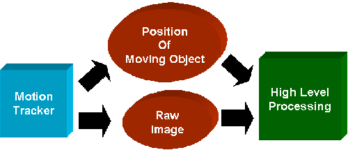
We designed the vision chip for detecting the position of moving object and obtaining the conventional video image simultaneously. The chip extracts the frame difference of image and computes the position of moving object in difference image by analog computation networks. Frame difference obtained at sensor level without additional computation and low-power analog networks can gives the cost effective solutions.
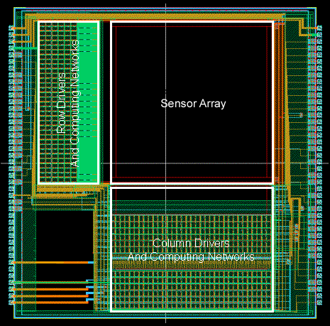 The key design concept of the sensor design is as follows; The sensor must provide the high quality video data additional to early processing results. This cancels out the need of additional sensor for image capturing used by higher level processing such as visual segmentation and recognition.


Results
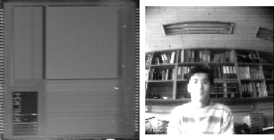
The following pictures shows the fabricated motion tracking sensor and obtained image from that chip. The motion tracking function in now in testing.
