


About
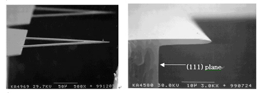
The AFM(Atomic Force Microscope) is not only a powerful tool for observing the surface topology with nanometer resolution but also a good candidate for various applications such as high density data storage and nano lithography. Typically, most of previous AFM probe tips have been made of SOI wafers using back-side anisotropic silicon etch. Therefore, the wafer cost is high and the dimension control is poor and the tip length and thickness are affected by variations in wafer thickness and etch rate. Instead of using buried oxide layer in SOI wafers as an etch stop in anisotropic etchant, heavily boron-doped layer can be used as an etch stop layer. With a heavily boron-doped cantilever realized in <100> silicon wafers, there is a silicon barrier at the backside of the cantilever as a result of anisotropic etch characteristics. Back-side alignment is essential in case of <100> and SOI wafers. By using <110> silicon wafers, probe tips are released in anisotropic etchant as the <111> face is located perpendicular to the cantilever.
Below pictures show the AFM probe tip fabricated using <110> silicon wafer with boron-doped cantilever and the enhanced view of the end of cantilever showing the (111) plane of the <110> silicon waver.
Related Publications
- Il-Joo Cho, Eun-Chul Park,Euisik Yoon,"AFM Probe Tips Using Heavily Boron-Doped Silicon Cantilevers Realized in a <110> Bulk Silicon Wafer" Digest Papers of Microprocesses and Nanotechnology, pp230-231,2000