Information
Recently, CMOS image sensors (CIS) have been widely used because they have many advantages compared with CCD in terms of on-chip signal processing capability, low cost and low power consumption. However, the image quality of CIS is poor owing to high dark current, low sensitivity, and high readout noise. Among these, the readout noise problem has been a major issue in CIS. There have been many efforts to reduce readout noise using various correlated double sampling (CDS) circuits. The CDS circuit can effectively remove fixed pattern noise (FPN), which is the dominant noise source of CIS, and they are adopted in most commercial CIS products. However, as the number of pixels becomes larger and the size of pixel gets smaller in multi-mega pixel CISs, it is difficult to accommodate column-parallel CDS circuits in a small column pitch.
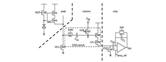
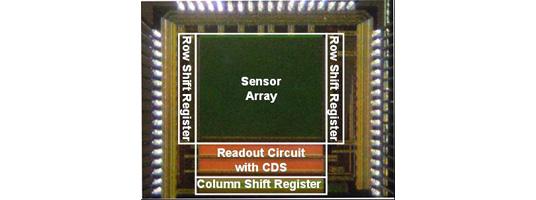
We proposed an area-efficient CDS circuit. Although most of the area of CDS circuits is occupied by two large on-chip sampling capacitors in conventional designs, proposed CDS circuit is devised using only one capacitor. The proposed CDS circuit has been successfully realized in a small two column pitch of 7.2µm in a test chip fabricated using 0.18 µm CMOS process and has demonstrated fixed pattern noise less than 0.46%.
We proposed an area-efficient CDS circuit. Although most of the area of CDS circuits is occupied by two large on-chip sampling capacitors in conventional designs, proposed CDS circuit is devised using only one capacitor. The proposed CDS circuit has been successfully realized in a small two column pitch of 7.2µm in a test chip fabricated using 0.18 µm CMOS process and has demonstrated fixed pattern noise less than 0.46%.
Figures

Figure 1. Readout Path of Proposed CDS Circuit


Figure 2. Chip Micrograph


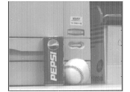
(a) CDS Not Applied

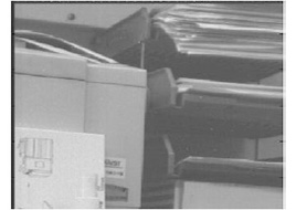
(b) CDS Applied
Figure 3. Sample Images

Related Publications
- S.-W. Han and E. Yoon, "Area-efficient correlated double sampling scheme with single sampling capacitor for CMOS image sensors," Electronic Letters, pp.335-336. Mar. 2006.


