Information
Charge Coupled Devices (CCD) and CMOS image sensors represent solid-state visible range photonic imaging devices that convert incident photons to electrical signals. CCD image sensors have been widely used for digital imaging systems such as digital video and still cameras because of their relatively high performance.
Although CMOS image sensor has the advantage of low power consumption, low cost fabrication, high speed readout, and system integration ability over CCD, it has not been widely adopted due to noise in pixel or readout circuit.
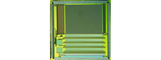
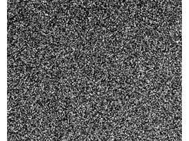
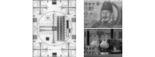
We have proposed and implemented 512 x 384 CMOS image sensor in 0.18-µm 1P4M technology with a 5.9 µm pixel pitch to compensate for kTC reset noise, image lag, and fixed pattern noise. A total of 330 µV(rms) random readout noise, which is a factor of two improvement over conventional reset operation, has been achieved. We can also suppress fixed pattern noise level to 250 µV(rms). The chip operates 1.8V and consumes 40 mW excluding I/) and off-chip DAC for a single slope ADC at 30 fps.
Figures

Figure 1. Chip Micrograph


(a) Image without Reset Control

(b) Image with Reset Control
Figure 2. Noise Suppression Using Reset Control


Figure 3. Sample Images

Related Publications
- Kwang-Hyun Lee, Euisik Yoon, "A CMOS Image Sensor with Reset Level Control Using Dynamic Reset Current Source for Noise Suppression," Technical Digest of International Solid-State Circuits Conference, pp.114-115. Feb. 2004.


