EXAMPLE:
DESIGN AND SIMULATION OF AN INVERTING AMPLIFIER
This example will help you familiarize with Design Framework II. You will
design a simple inverting amplifier, and then observe its operating point and
frequency response behavior. This will show the most important commands and
steps to use when working with schematics in DFII.
Before starting with the design example, there are some details that are worth
mentioning:
- The appendix contains some notes about using the on-line help feature, and using the mouse. There's also a table with keyboard shortcuts.
- Most of the commands in DFII can be accessed in multiple ways: pull-down menus, shorcut keys, buttons in toolbars, etc. In the described example, all the commands are referenced by their position in the pull-down menus.
- The most used key in DFII is ESC. It is used to cancel on-going commands.
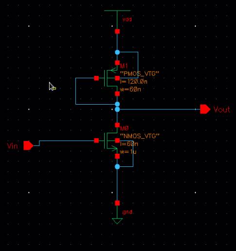
The following picture shows the common source amplifier circuit, ready for netlisting. The next section explains how to draw it in DFII. The common source amplifier circuit with diode connected load (the PMOS) is described in section 3.2.2 of Razavi’s book.

Figure 1: Design example.
1.
Create a library for your new design:
From the library manager window:
File->New->Library
Type a new name, such as TEST.
Under
the heading "Technology File", choose "attach a
existing techfile".
Then from the dropdown menu choose "NCSU_Techlib_tsmc03d Click OK
2. Create a new
cell, where you will design the inverter:
In Library Manager:
Highlight your new library (TEST if that is what
you chose).
File->New->Cellview
Choose library TEST, cell name "inverter", view name
"schematic", and Tool "Composer-Schematic". Click OK.
3. Design your
circuit:
3.1
Placing components:
Useful Cadence shortcuts:
I – add instance
Q – edit component properties
M – move component
C – copy
U – undo
[ or ] – zoom
W – draw wire
P – place pin
L – label wire
For
this inverter, you will need an nmos transistor, a pmos transistor, and power and ground nodes.
From Schematic window:
Add->Instance
Add Instance and Component Browser windows will open.
Make sure the Library in the Component Browser is set to NCSU_Devices_FreePDK45.
Click on
‘Browse’ to open the component browse, and select the NMOS_VTG
transistor. Edit the width and length parameters.
If you would like to place resistor, inductor or capacitor components for future designs, use components from library AnalogLib.
Also, from the AnalogLib, get the symbols for vdd and gnd (they define the net names for the power and ground nodes).
If you make any mistake, you can always use:
Edit->Delete or
Edit->Rotate or
Edit->Move or
Edit->Stretch
You need to change the properties of some components:
Edit->Properties->Objects
Select the transistor, and change the following parameters:
Width: 1u
Length: 60n
Make sure you change the Width and Length boxes to these values,
not the Width(grid units) and Length(grid
units) boxes.
Place the PMOS
transistor. Set the dimensions as described below:
Width: 120n
Length: 60n
3.2
Connect components:
Connect the component terminals as shown in figure 1, using:
Add->wire (narrow)
The shortcut for adding wires is ‘w’.
4.
Adding Pins:
By adding pins, you can identify the I/O ports of the schematic. At a later stage, you can also use pins as connection points for hierarchical designs. To learn more about this, see the section about creating symbols.
Add->Pin
Type the pin name, such as Vin, select the
direction as "input", and place it in the schematic. Do the same for Vout, selecting the direction as "output".
5.
Simulate:
From analogLib, get your
signal source. You can find anything you need for this project (and much more),
in there: vdc, idc, vpwl, vsin, vpulse,
etc. For this example, let's get vdc, and connect it
to the gate of the transistor.
Edit the properties of vdc so that it supplies a DC
voltage of 600 mV, and an AC magnitude of 1 V.
Get
another vdc from analogLib,
and connect it to vdd! and gnd!. You can place more vdd! and gnd! symbols
since they are global (that's what the exclamation mark '!' means).
Edit the properties of vdc so that it supplies a DC
voltage of 3.3 V.
We will also add a load capacitance, simulating the capacitance of the next stage. Place a capacitor between the output and ground of 1pF. Your schematic should now look something like this:

Figure 2: Schematic ready for simulation.
In Schematic Window:
file->Check and Save
There should be no errors. Warnings such as "Solder dot on cross
over" are okay.
Launch->ADE L
In
Cadence Analog Design Environment:
The following two steps only need to be done for this first session.
Setup->Simulator/Directory/Host
Set the simulator to Spectre.
Setup->Model Libraries Use the model files in the directory (for VLSI lab):
/home/class/(x500)/FreePDK45/ncsu_basekit/models/hspice/tran_models/models_nom/
Select the models for the components you are using (i.e. PMOS_VTG and NMOS_VTG) and OK.
Set Analysis:
Analyses->Choose
Select dc analysis
Click "dc operating point"
Select ac analysis
Choose sweep range, from 1 k to 1 G.
Choose sweep type "logarithmic, 10 points per decade.
Click OK.
Choose nodes to be saved:
Outputs->Save all, click 'OK'.
Start simulation:
Simulation->netlist and Run
The simulator status can be seen in the log (CIW) window. Ignore the warnings about the model files, and wait until it finishes.
6. View Results:
To see the operating point, do the following in the Analog Artist Simulation Window:
Results->Annotate->DC Node Voltages.
The node voltages will be annotated in the schematic window. You can also annotate the transistors operating points by choosing:
Results->Annotate->DC Operating Points.
To
see the results of the ac analysis, do the following:
In the Analog Artist Simulation Window:
Tools->Calculator
Then, in the Calculator:
Click the "vf" button,
click on output net in schematic.
Click "plot".
The Waveform Window opens. You can find, for example, the unity gain frequency easily by choosing:
Markers->Horizontal Marker
Type 1 Volt in "Marker locations", and click "Apply". If
you want to see the exact value, click "Display Intercept Data".
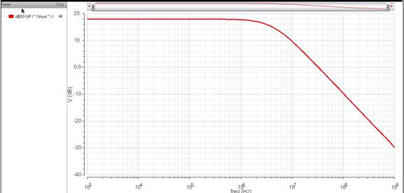
You can also see the output voltage in dB. Just click the 'dB20' button in the calculator, and then 'Plot'. To delete other plots, click directly on the curve and press Delete.

Figure 4: AC analysis results